Porous Silicon
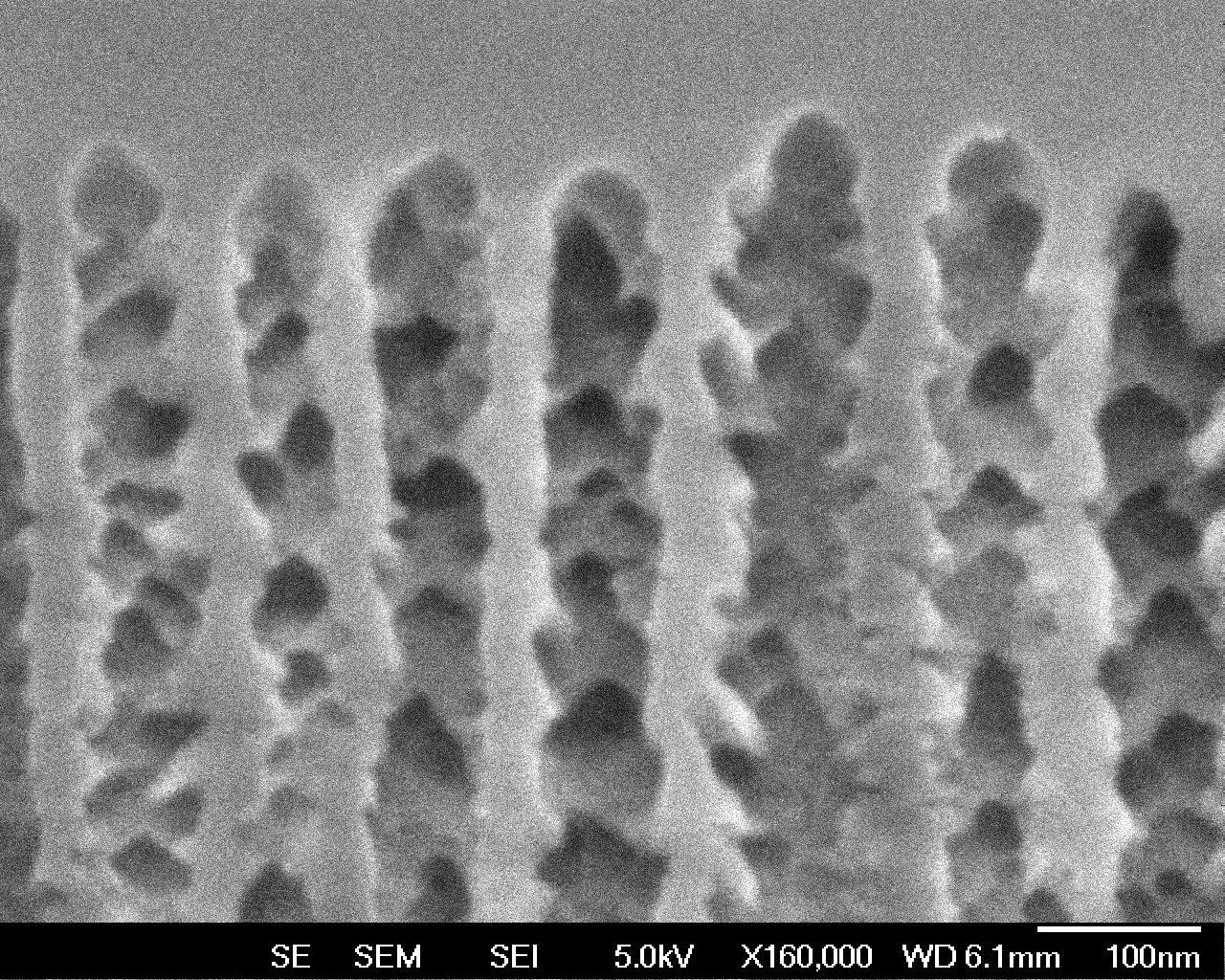
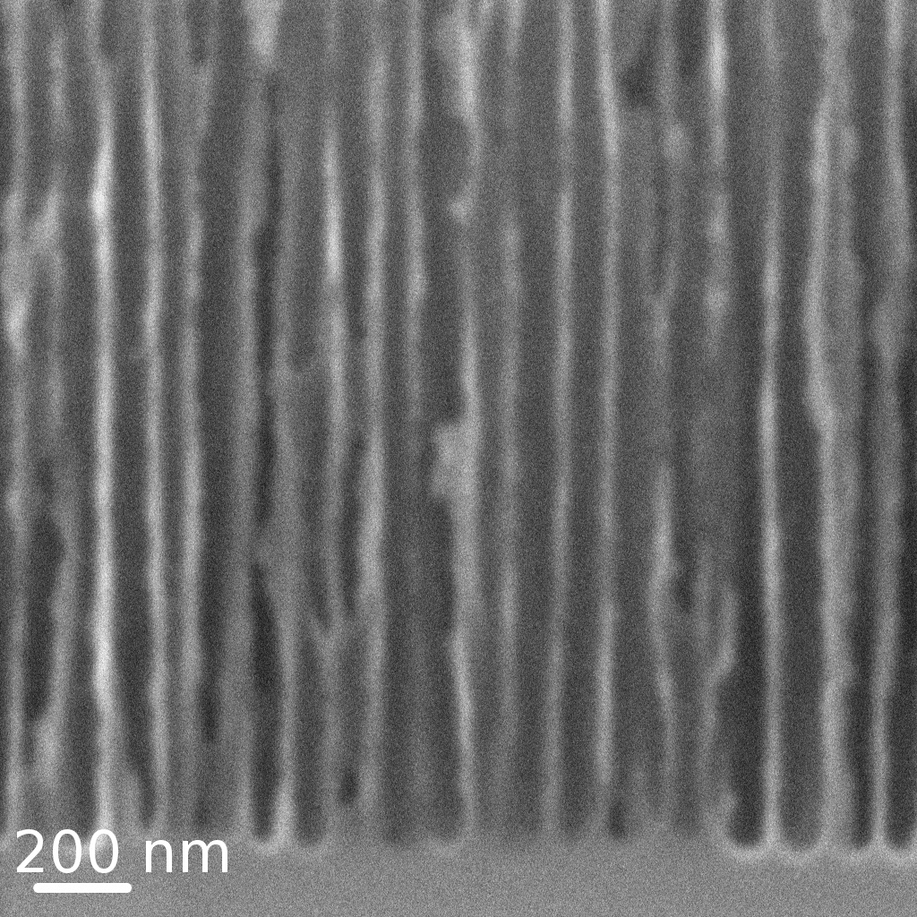
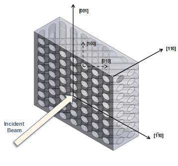
Porous silicon is obtained by electrochemical etching of bulk silicon in fluoride containing solutions.
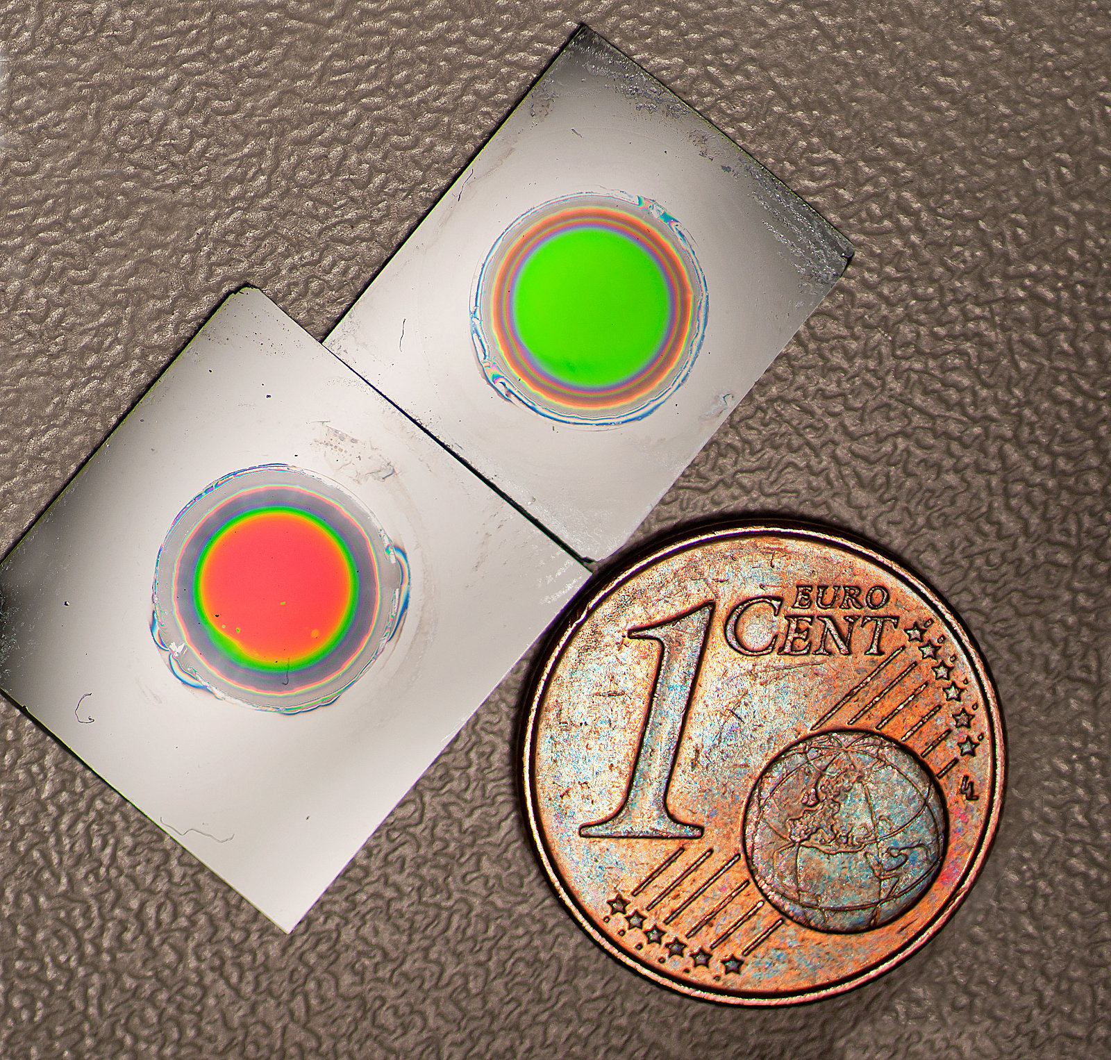
It was firstly described in 50's and found microelectronic applications as sacrificial layer. The interest on this material raised only after the discovery of its bright photoluminescence (late 80's). In search for increase it luminescence efficiency researcher develop techniques to modulated the Porous silicon porosity to fabricate dielectric mirrors and cavities that enhance light extraction efficiency. At the same time its huge surface area suggest possible applications in sensing. By combining the high optical quality of the porous structures achievable and the large specific area it was possible to 'fabricate highly sensitive devices based on optical and electrical responses.
Today porous silicon encompass a broad classes of structures, ranging from truly nanometric scale up to micron sized pores. This large tunability of its the typical length scale and the well known surface functionalization chemistry enable the possibility to fabricate free standing porous membranes to be used as the basic building block of highly sensitive devices.


