Laboratory Equipment
Our laboratory is dedicated to the growth and characterisation of semiconductor materials in view of its use on photonic applications. We can grow II-VI, III-VI and other compounds. Currently our interest is on oxides as ZnO, CdO, MgO, Ga2O3, In2O3 and their alloys.
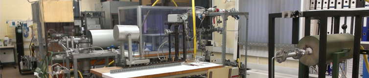
We have a wide variety of facilities for crystal growth and sample characterisation. Next you can see a partial instrument list and take a look at some photographs of our laboratory equipment.
Material Preparation and Handling
- Ion Milling Machine, provided with an Ar ion gun
- Cutting Machine, consisting of a diamond wire saw
- Mechanical Polishing Machine, equipped with an integral abrasive auto-feed system
- Ultrasonic disc cutter
Crystal Growth Lab (Lab. -1.23)
- Evaporation System for Thin Film Vacuum Deposition
- Thermal Treatment Oven with Quartz Vessel and Vacuum System
- Vacuum System For Ampoules
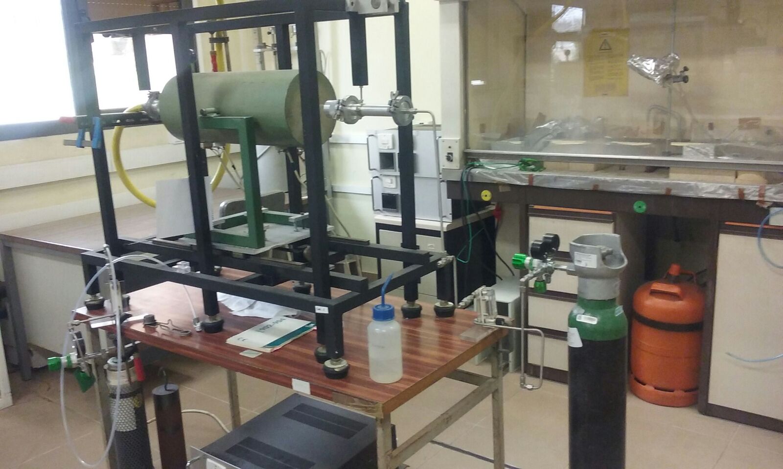
- Czochralski Furnace
- THM Furnaces
- Two Zones PVT Horizontal Furnaces
- Four Zones Bridgman Horizontal/Vertical Furnaces
- Seven Zones Horizontal Furnace
Crystal Growth Lab (Lab. 0.10)
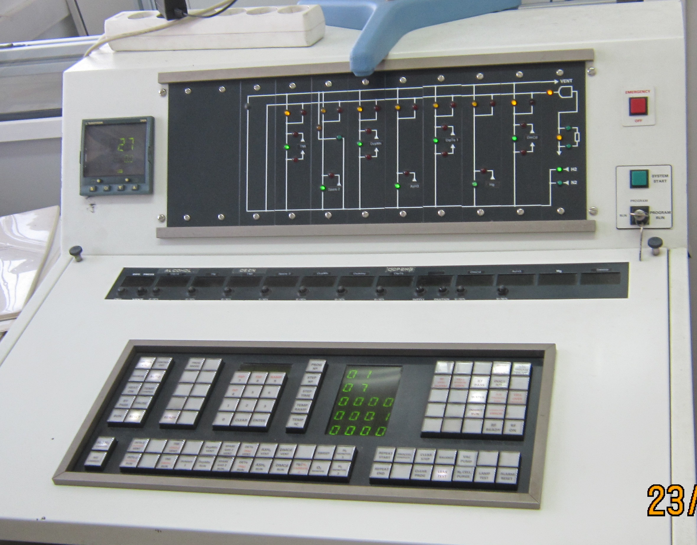
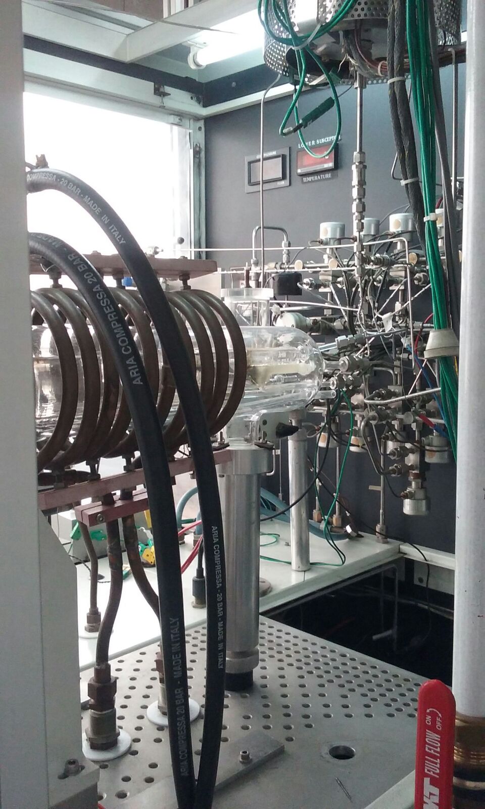
- Two-Inlet Vent-Run Type MOCVD Reactor (Quantax 226 Refurbished by EMF Ltd), Reactor Cell Cabin
- Cooling Baths With Precursor Blubbers
- Control Console
- Rapid Thermal Annealing
- Mass Flow Controlers
Crystal Growth Lab (Lab. 2.51)
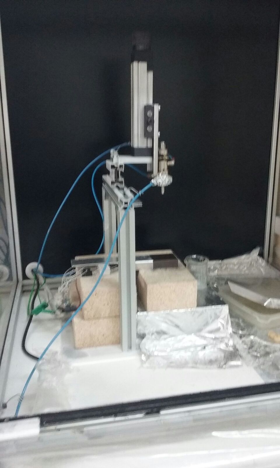
- Spray Pyrolysis Growth Systems
- Magnetic Stirrer
- Ultrasonic Cleaning System
- Syringe Pump
- Peristaltic Pump
- Mist-CVD (Chemical Vapor Deposition)
Characterisation Techniques
- X-Ray Diffraction Facilities (Powder and Epitaxial Layers
- SEM and TEM facilities
- Optical analysis (UPM)
- Electrical analysis (UPM)
- Optical modeling (UPM)
- Raman (GEO3BCN)
- Cathodoluminescence (UVA)
Processing Techniques (UPM)
- Crestec Electron Beam Nanolithography (Crestec)
- UV Photolithography
- Inductively Coupled Plasma Etching (ICP)
- Reactive Ion Etching (RIE)
- Metal Deposition
- Ultrasonic and Thermocompression Microsoldering
- Conventional post-growth heat treatment
More:
|
|
|
|
|
|