Laboratories
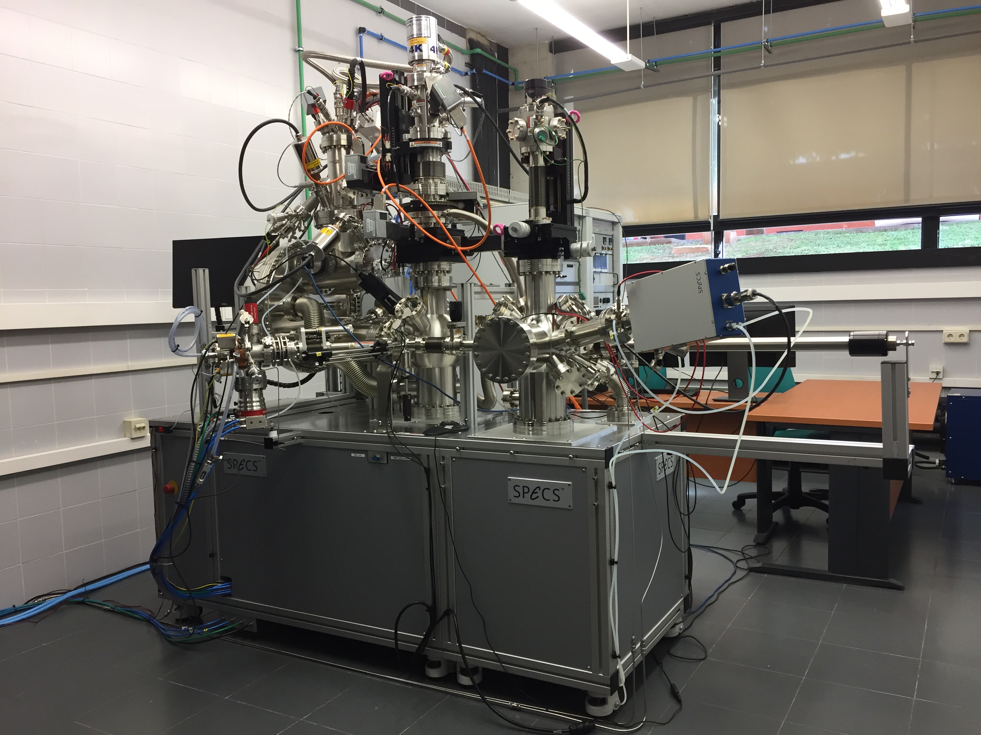
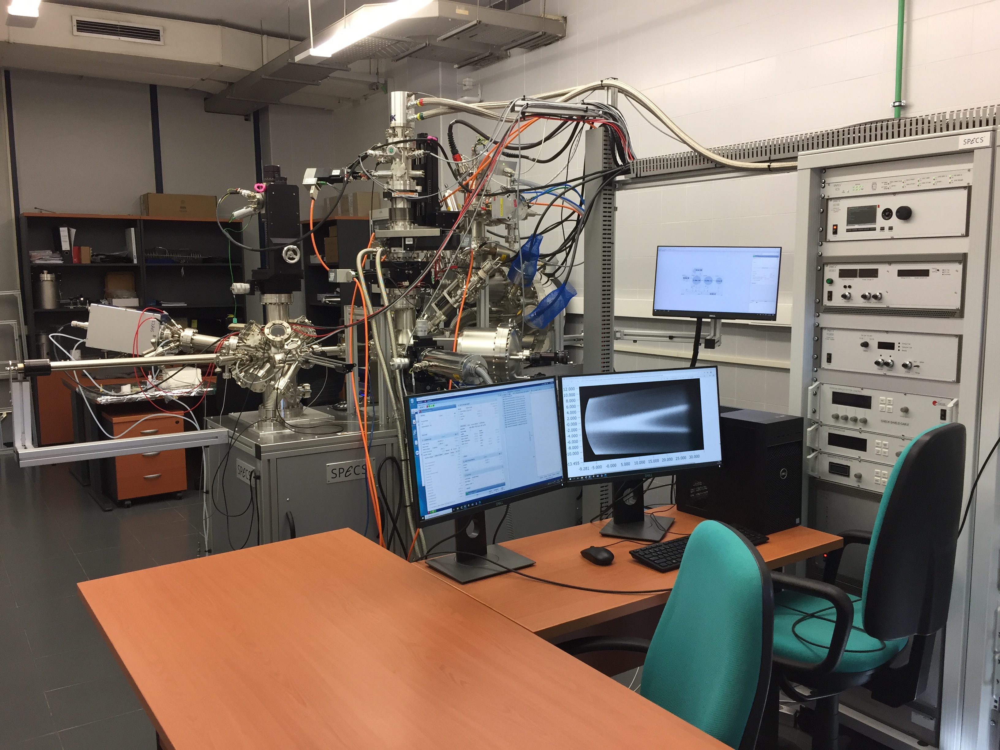
Since November 2020, a high-performance Photoemission system from SPECS GmbH is operative in our Quantum Matter Laboratory (QMatter), able to carry out high-resolution angle-resolved photoemission (ARPES) and x-ray photoemission (XPS). A time-lapse movie of the installation process can be found here below or directly in the web.
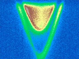
The photoemission system is currently equipped with an ASTRAIOS 190 2D-CMOS/3D-Spin VLEED Detector, which allows for a fully 3D characterization of the photoelectron spin. The UV source is a UVS 300 VUV Source. The x-ray source is a Monochromated X-ray source µ-FOCUS 500 (with an Al x-ray anode). The analysis chamber also has an electron gun for charge compensation, which allows to measure insulating samples. The 5-axis sample manipulator of the equipment, with heating and He closed cycle cooling systems, allows to perform photoemission experiments at temperatures between 7 and 1000 K. State-of-the-art complements are incorporated, such as Flood Gun, a hybrid Hydrogen/Nitrongen/Oxigen plasma source, a LEED system, and a double electron beam evaporator (this, from Tectra GmbH). The manipulator of the preparation chamber is equipped with heating and N open-cycle cooling systems that allows to perform samples treatments between 100 and 1000 K.
This system is one of the few 3D spin-resolved photoemission equipments existing in the world. The figure included here below provides for a wide perspective of the ARPES equipments existing in the world and the XPS existing in Spain. Use the menu of the map to select different options.
Researchers acknowledge funding from the University of Valencia, the Generalitat Valenciana, and the European Union, through FEDER founds (Project: Determination of the electronic and chemical properties of nanomaterials by XPS-ARPES-SRPES, Ref.: IDIFEDER/2018-055).

![]()
Other LabsBesides, synthesis, sample treatmets, and a complete optoelectronic characterization of materials and devices can be performed in the laboratories of the Optoelectronic and Materials and Devices (UMDO) research unit.
As well as those of the Photonics & Semiconductors group.