LFNN
LFNNIt provides laser ablation, cleanroom based microfabrication complemented by our external collaborators facilities, for the fabrication of plasmonic and photonic based devices and materials.
We are working on various nanotechnology research lines. Here we summarize in more detail the systems and devices that we are working on.
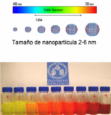
- By physical (ablation in liquid phase) and chemical methods of III-V (GaAs, InAs) and II-VI (CdS, CdSe, PbSe) semiconductor nanocrystals (2-10 nm in diameter) with absorption edges from the near infrared to UV. In the latter case the quantum dots (see below) are obtained with high optical quality.
- InAs quantum dots by Pulsed Laser Deposition under conditions of Ultra-High-Vacuum for optoelectronic devices.
- Metal nanoparticles (5-25 nm in diameter) of Ag, Au and Ag-Au alloys by means of chemical synthesis produced by laser ablation of a suitable target. This method has been patented for their novelty.
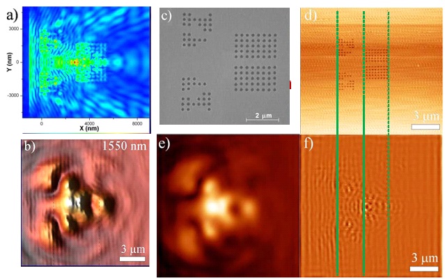
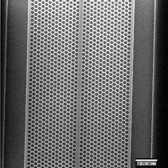
- In the field of manufacturing we have designed, fabicated and characterised an integrated Si NIR photonic lens focused on a photonic crystal (see image below). a) FDTD-3D simulation of the electric field intensity of 4 nm on silicon, b) SNOM image directly to the device at 1550 nm, c) SEM of the device, d) recorded with the SNOM topography, e) diffracted waves in air obtained by filtering the image b, f) waves.
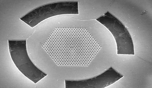
- Based on previous work by Dr. Lorenzo, several designs were prepared for making 2D photonic crystal cavities in GaAs with high-index incrustations in order to validate results achieved in work prior to the aforementioned work. In the figure below a membrane in GaAs design can be seen to have been fabricated.
- One of our first photonic structures can be seen below, a photonic double-heterostructure cavity.
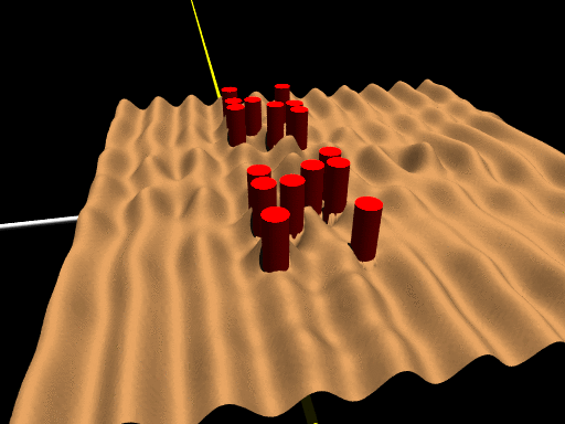
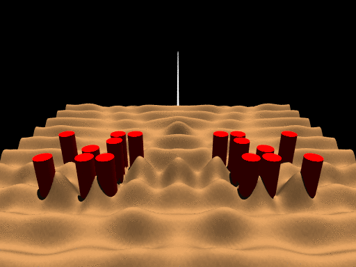
- Inverse design is having a growing importance in Physics as a means to obtain structures with specific functionality. This type of design includes algorithms based on iterative modification of an original structure gradually improving their effectiveness. Among others, we can find those based on natural selection (Genetic algorithms) or the cooling of a crystal (Simulated annealing). In particular, the inverse design is of great use in the physical processes related to the scattering of waves by objects of some complexity.
- To perform such optimizations it is needed a large computational power and a detailed theoretical description of the process of scattering of waves by what is required to handle concepts in parallel computing and wave theory. Thus, for example, scattering theories are used to describe the process experienced by waves impinging on objects made of many individual objects.
- The algorithms used alter the geometric arrangement, intrinsic characteristics and shapes of these objects in order to obtain the desired result. The three types of classical waves of interest are acoustic waves, electromagnetic waves and electron waves on the surface of metals (plasmons). First, the inverse design uses sound waves to lens design with potential applications in ultrasound (non-invasive surgery and ecography) or environmental acoustics. Electromagnetic waves can be used in the design of antennas or, at optical frequencies, in the design of photonic crystal structures (single photon sources, waveguides, couplers, lasers and photovoltaics among many others). Finally, with regard to electromagnetic waves in two-dimensional surfaces, it can be found novel applications in the field of plasmonics or graphene material devices (see animations).
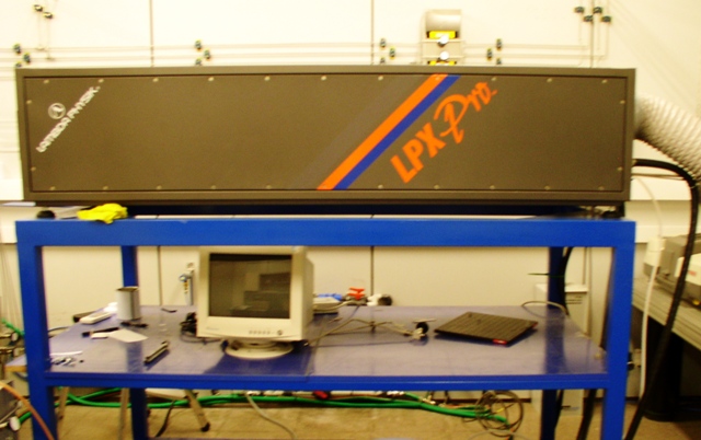
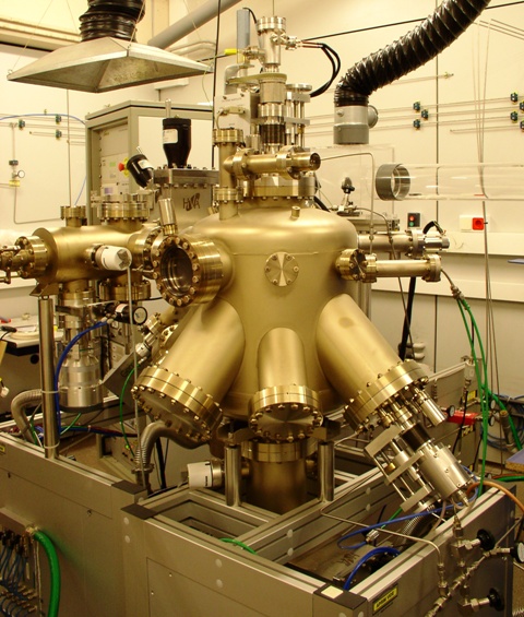
- Excimer laser 193 nm (400 mJ).
- UHV chamber for laser ablation. The equipment has water cooling, and inlets for gases (Ar, N2, He, H2) to the UHV chamber and F-Xe to the excimer laser.
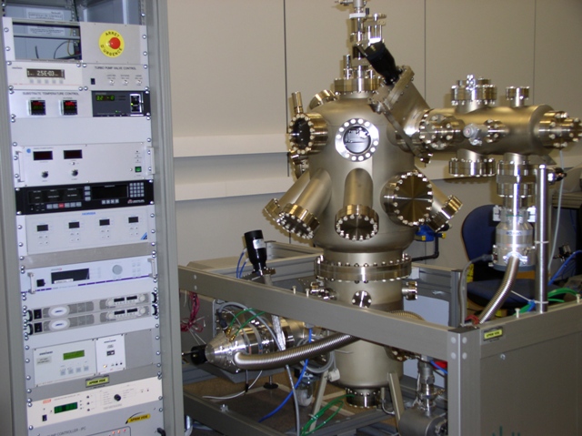
- UHV sputtering chamber (2" and 3" ports). The equipment has water cooling and inlets for carrier gas (Ar) or potentially others (N2, O2, ...).
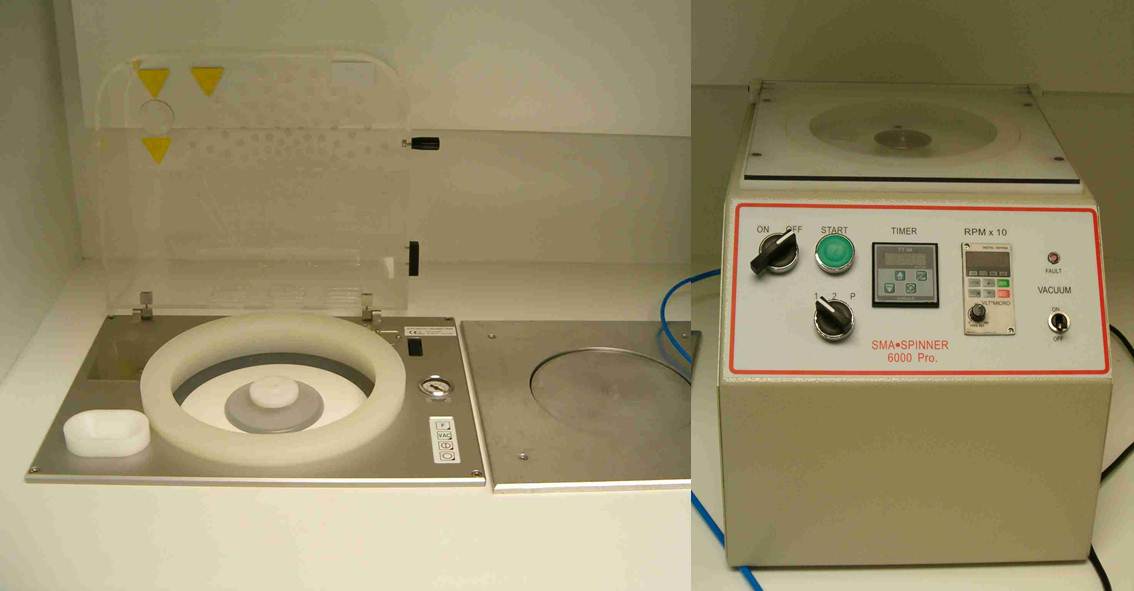
- Spin coaters. For precision control deposition of homogenous layers of polymers, resists and nanocomposite materials.
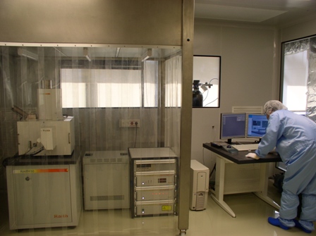
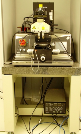
- Raith 100 Electron Beam Lithography. A system for marking patterns for later etching as a device, with a resolution of 50 nm. This valuable system is based on an electron microscope column that allows focusing the electron beam in a specimen with interferometric positioning with an accuracy of 1 nm. In addition, the vacuum chamber is designed to be configured as a nanotechnology station, which it will be upgraded to in successive stages of improvement and expansion of research lines.
- UV Lithography setup. Requires just a nitrogen (or dry air) and vacuum for sample holding.
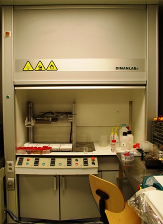
- Wet etch facility. For etching lithographically patterned samples.
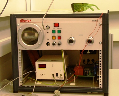
- Oxygen plasma cleaner (asher) The machine has inputs for oxygen and nitrogen for cleaning wafers and samples prior to further processing.
- Microsolderer. For bonding components within microelectronic circuits.
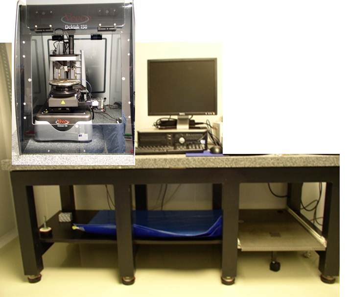
- Profilometer. For determining thin film thicknesses in 2D.
Estimated Global value: ~1.200.000 €
News & Events Environment