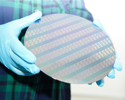
In the last decades, innovative semiconductors have emerged from molecular materials to inorganic. Some of them have demonstrated properties that allow their use in advanced electronic devices such as transistors, photodiodes, light emitting diodes and photovoltaics. In this project, we focus on the the metal-halides of perovskites, because they have demonstrated excellent cargo carrier mobility when processed in thin sheets. However, the processing of innovative semiconductors is limited to complicated methods, expensive and low speed, such as molecular beam epitaxy or similar processes using high vacuum.
Acronym
P3
Reference code
TSI-069100-2023-0012
Description
The main objective of PROSEM is to develop a method and deposition process that enable high-quality, large-scale and high-speed semiconductor preparation.
The purposes will be the following:
- To develop a solvent-free process using fast steam sublimation to achieve deposition rates above 500 nm/min with good reproducibility and high uniformity.
- The integration of semiconductor films in proof-of-concept devices, such as transistors, photodetectors, photovoltaic diodes and light emitters.
- Microstructure semiconductors and their integration into microelectronics.
Developers of the project
Institute of Molecular Science
Principal investigators:
- Bolink, Hendrik Jan
- PDI-Catedratic/a d'Universitat
Start date
2024
May
End date
2028
May
Funding agencies:
Ministry for Digital Transformation and the Civil Service, European Union Recovery, Transformation and Resilience Plan, «European Union - NextGenerationUE»
Grant under the European Recovery, Transformation and Resilience European Plan, financed by UE, NextegenerationEU.
Project financed by the State Secretariat for Telecommunications and Digital Infrastructure. Referencia TS-069100-2023-0012.
Partners:
OXFORD PHOTOVOLTAICS LIMITED
![]()
Project type
- EU - NextGenerationEU