P7
TSI-069100-2023-0012
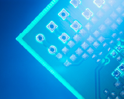
X-ray detectors based on photon counting are being gradually integrated into the latest generation of systems for medical diagnosis, industrial inspection and security. These detectors consist of two types of interconnected semiconductor pixelated devices: a sensor and a photon counter chip.
Applications that require the detection of high-energy photons need high atomic number sensors based on, for example, II-VI semiconductor compounds or materials with a perovskite structure. The fundamental properties and fabrication techniques of these materials are less well known than those of semiconductors such as silicon or germanium, traditionally used in the microelectronics industry.
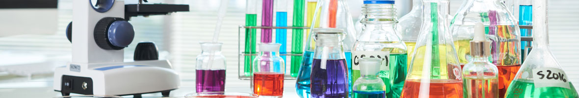
The relative lack of maturity in growth and microfabrication processes of these materials (e.g. CdTe, CdZnTe, Pb-Perovskites) results in low-yield and high-cost processes. Defects related to stress accumulated during growth, lack of homogeneity in transport properties and high leakage currents are commonly associated with problems occurring during the sensor production process. For these reasons, it is necessary to make a quality assessment before and during de complex detector fabrication process.
When scaling up the production volume of these high atomic number sensors,
a thorough understanding of their fundamental properties is required. In particular, when controlling production costs, metrology tools and procedures must be developed to track the most critical properties of the sensor at each step of the production line.
- Mariñas Pardo, Carlos
Ministry for Digital Transformation and the Civil Service, European Union Recovery, Transformation and Resilience Plan, «European Union - NextGenerationUE»
Grant under the European Recovery, Transformation and Resilience European Plan, financed by UE, NextegenerationEU.
Project financed by the State Secretariat for Telecommunications and Digital Infrastructure. Reference TS-069100-2023-0012.
DECTRIS Ltd
![]()
- EU - NextGenerationEU