- Universitat de València
- Bolink, Hendrik Jan
- PDI-Catedratic/a d'Universitat
- Nathan Jacques Rodkey
- Bas Antonius Hendrikus Huisman
The preparation of uniform thin films without the use of solvents is crucial for a wide range of applications, ranging from coatings to semiconductor devices. Typical semiconductor-based devices are, transistors, light emitting diodes and solar cells. In order to prepare high performance coatings, LEDs and solar cells, homogeneous films are needed.
Processing methods to prepare perovskite thin films are via solution-based processes that need to use coordinating solvents to dissolve the inorganic precursors salts and via vacuum-based processes that are solvent free processes and widely used in industrial application. Both methods have limitations. Coating from solutions due to the need to use coordinating solvents to dissolve the inorganic precursors salts. These solvents, such as dimethylformamide (DMF) or dimethylsulfoxide (DMSO) have a high boiling point which makes it difficult to completely remove them from the finished film.
The development of perovskites with vacuum-based technologies has not been straightforward. This is largely due to the organic compounds involved in the process (e.g. methylammonium (MA) and formamidinium (FA) salts), which are needed to give the highest efficiency devices. Prolonged heating of these organic salts close to their sublimation temperatures leads to their decomposition. In an industrial tool, this would severely limit the production yield and make the process uneconomical. The complexity of perovskite compositions, and the number of compounds found in high efficiency cells, has increased over the last years. Controlling these sublimation sources reliably over long durations of time is very challenging. Thus, there is still a need to find a production method of thin layers of perovskite suitable for industrial processes.
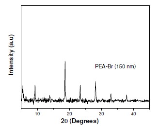
Researchers from the Universitat de València have developed a new process to obtain thin films by a vapour evaporation method that overcome the disadvantages of the vapour evaporation process by decoupling the heating of the source from the presence of the powders. Also, a special apparatus that enables the controlled supply of the powders into a pre-heated crucible inside a high vacuum chamber has been designed. This enables to deposit smooth perovskite films with thicknesses above 100 nm that are used to prepare solar cells and light emitting diodes.
By introducing powder incrementally, in μg quantities, the invention is able to address the problems of rampant sputtering, competing degradation pathways, and limited film thicknesses that current flash evaporation processes are combatting. In this way we are able to report the formation of perovskites with as many as six components, as a single-source, sputter-free process, and demonstrate their performance in devices.
The invention is applicable in semiconductor devices manufacturing such as solar cells, transistors and light emitting diodes.
The method of the invention has the following advantages:
- Production of uniform and smooth hybrid organic-inorganic perovskite films.
- Production of thin films of materials that consist of multiple components each with a different sublimation temperature.
- It is simple and rapid, so lower production costs and faster device fabrication is feasible.
- Patent granted
Blasco Ibáñez Campus
C/ Amadeu de Savoia, 4
46010 València (València)