The crystal growth group of the Universitat de València focuses its activity on the growth and structural and morphological characterisation of semiconductors, both in volume and in the form of layers and nanostructures. This activity has been carried out mainly within the framework of different research projects in the area of materials for optoelectronics and spintronics. The results obtained have been reflected in a significant academic contribution both in articles in journals of wide scientific dissemination and in congresses and workshops.
The approach to the technological sector has been carried out in two areas: solar energy and humidity and infrared sensors. For the development of this research activity, a laboratory has been set up in which different crystalline growth techniques have been installed: Bridgman, Physical Vapour Transport, Travelling Heater Method, MOCVD, Spray Pyrolysis, Hydrothermal; as well as different preparation techniques and post-growth treatments, which provides a wide range of infrastructures and development possibilities.
In relation to structural and morphological characterisation, the members of the group have proven expertise in high-resolution X-ray diffraction (HRXRD) and high-resolution transmission electron microscopy (HRTEM). The correlation of material properties with growth conditions has allowed a better understanding of growth processes and structural defects and is the focus of the main part of the group's work. At present, a large part of the activity is focused on the oxides of group II materials (ZnO, CdO and MgO) and their alloys.
Within this framework was the leadership of the European SOXESS project as well as the organisation of Symposium IX at the E-MRS on this topic. The group collaborates on a regular basis with national groups (Uno.Valladolid, Uno. País Vasco, Instituto Jaume Almera, (ISOM) UPM, as well as with foreign groups (CNRS-Bellevue, France; University of Warwick, UK; National Renewable Energy Lab. in Golden, Colorado, USA).
Crystal growth and characterisation of materials for UV optoelectronics and spintronics.
- Structural characterisation
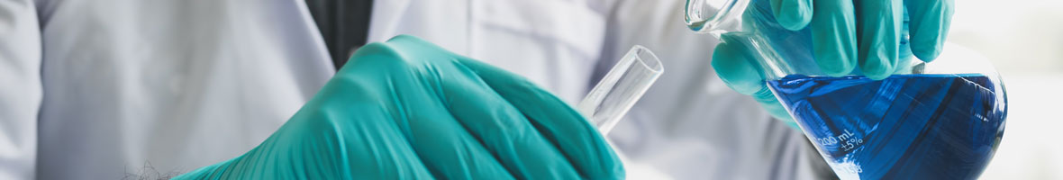
Characterisation using high-resolution X-ray diffraction (HRXRD), X-ray multiple diffraction (XRMD), scanning electron microscopy (SEM), high-resolution transmission microscopy (HRTEM). The materials analysed can be bulk, layered or nanostructures.
- Crystal growth
Growth of materials using the techniques of: Bridgman, travelling heater method (THM), physical vapor deposition (PVD), metalorganic chemical vapor deposition (MOCVD), spray pyrolysis (SP). Currently, different types of oxides (CdO, MgO, ZnO and alliatges) are being grown.
- Physical properties
Characterisation of physical properties, with special emphasis on optical properties: absorption, photoluminescence, Raman spectroscopy.
- MUÑOZ SANJOSE, VICENTE
- PDI-Catedratic/a d'Universitat
- AGOURAM OUHTIT, SAID
- PDI-Ajudant Doctor/A
- ATENCIA HENAREJOS, ANTONIA
- PIT-Investigacio Escala Tecnica Basica
Partners
- Luis Artus Surroca - Consejo Superior de Investigaciones Científicas (Madrid)
- Ramón Cusco Cornet - Consejo Superior de Investigaciones Científicas (Madrid)
- José Ángel García García - Universidad del País Vasco
Burjassot/Paterna Campus
C/ Dr. Moliner, 50
46100 Burjassot (Valencia)
- MUÑOZ SANJOSE, VICENTE
- PDI-Catedratic/a d'Universitat